SELECTED WORK / PROJECT 004

RMS to DCAnalogue signal-processing circuit

Designing, simulating and testing an analogue circuit that estimates RMS voltage as a DC output.

Analogue electronicsCircuit designLTspiceBreadboard prototypingBench testing
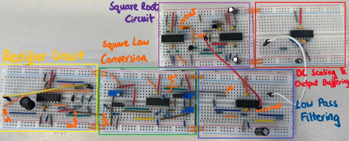
Annotated breadboard prototype showing the rectifier, square-law, low-pass, square-root and output stages
RMS-TO-DC / BREADBOARD PROTOTYPEPERSONAL PROJECT · PROTOTYPE HARDWARE
MY ROLE
Circuit design & testing
CONTEXT
Personal electronics project
TOOLS
LTspice · Analog Discovery 2
BUILD
Modular breadboard prototype

01 / THE CHALLENGE

Measure the signal.
Keep the meaning.

Convert a small input waveform into an analogue output representing its root mean square voltage.

  • I undertook this personal electronics project to explore analogue signal processing.
  • The circuit used precision rectification, nonlinear conversion and filtering to process different waveform shapes.
  • LTspice simulations informed the design before breadboard construction and bench testing.
±5 V

Design supply rails

100–200

mV peak-to-peak input range

10 kHz

Upper design frequency

Design targets; testing exposed a substantial limitation at 10 Hz.

02 / REQUIREMENTS & SYSTEMS

A calculation,
built from circuits.

  • The main signal path implemented squaring, averaging and square-root conversion.
  • Each stage needed compatible signal levels and sufficient isolation from neighbouring stages.
  • Available kit components and the AD2 power supply constrained the practical design.

DESIGNING TO SPECIFICATIONS

Criteria that shaped the prototype

  • Power: Operate from ±5 V rails with a circuit-current target of no more than 200 mA.
  • Signal range: Handle 100–200 mV peak-to-peak inputs and frequencies from DC to 10 kHz.
  • Waveforms: Consider sine, square, triangle and complex signals with crest factors from one to three.
  • Input loading: Target at least 1 MΩ input impedance and no more than 50 pF input capacitance.
  • Accuracy: Aim for a 5–10% output-error allowance.
  • Response: Target a settling time below ten seconds.

These are design targets; performance across the full range remains unverified.

03 / CIRCUIT DESIGN & SIMULATION

From schematic
to signal response.

Stage-level simulation helped expose scaling and loading issues before integration.

Overall circuit topology

Connect the stages deliberately

  • The main path linked the rectifier, squarer, low-pass filter and square-root circuit.
  • Buffers reduced interaction between circuit stages.
  • A separate DC path and output summing stage explored offset handling.

04 / SIGNAL-PROCESSING STAGES

Designing
each transformation.

  • The design divided the RMS calculation into stages that could be simulated, built and inspected separately.
  • Small internal signal levels made amplifier offsets and gain selection particularly important.

SIGNAL STAGE 01

Precision rectifier

  • Op-amp feedback compensated for diode voltage drop when rectifying the small input signal.
  • The half-wave stage and summing amplifier produced full-wave rectification.
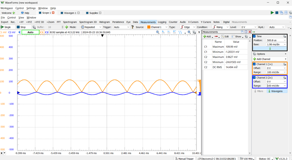
  • Bench traces showed a switching glitch linked to non-ideal amplifier behaviour.
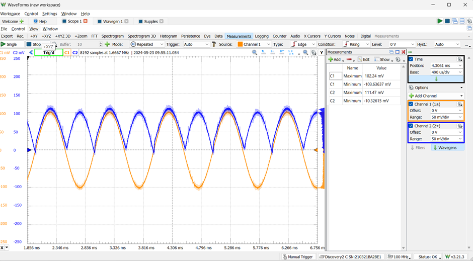
View rectifier bench traces
Precision rectifier schematic

SIGNAL STAGE 02

Square-law conversion

  • A logarithmic amplifier, gain stage and antilog amplifier implemented the square-law operation.
  • Resistor selection set the conversion scale.
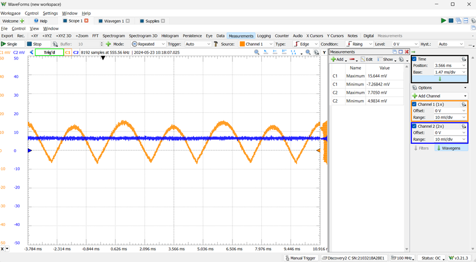
  • Offset trimming became essential because the stage’s output was only a few millivolts.
View square-law bench traces
Square-law circuit

SIGNAL STAGE 03

Low-pass averaging

  • An RC low-pass filter smoothed the squared signal towards its average value.
  • An op-amp buffer isolated the filter from the next stage.
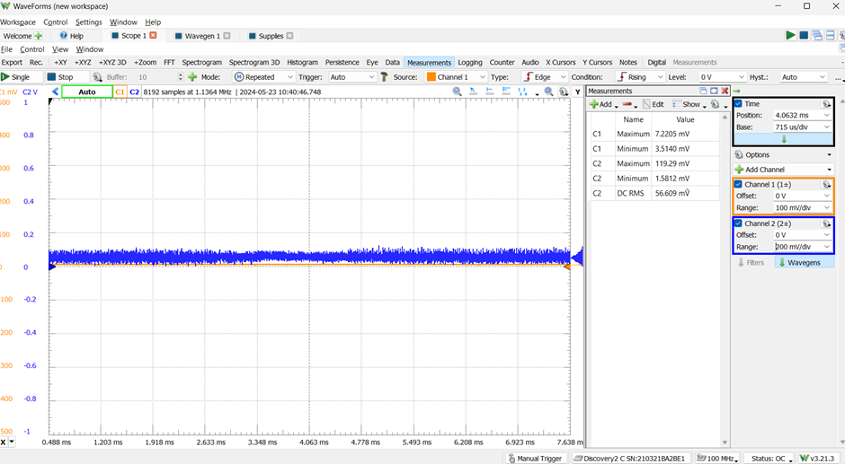
  • The filter choice connected output ripple with the converter’s response time.
View filter bench traces
Averaging filter

SIGNAL STAGE 04

Square-root conversion

  • The square-root stage reused the log/antilog principle with a different intermediate gain.
  • Its resistor values were revised to suit the smaller signal arriving from the averaging filter.
  • Bench testing checked the final nonlinear stage before evaluating the whole converter.
View square-root bench traces
Square-root circuit

05 / DESIGN ITERATION

Simulation meets
component reality.

  • Rectification: The initial diode-bridge idea gave way to a precision rectifier for small-signal accuracy.
  • Topology: Log/antilog circuits were selected over more complex multiplier alternatives.
  • Offset trim: Potentiometers were added to compensate for op-amp offsets in the nonlinear stages.
  • Power draw: Higher-value trim resistances reduced the load imposed on the supply rails.
  • Stage scaling: The square-root circuit was adjusted for the filter’s smaller output signal.
  • Component values: Series resistor combinations achieved values unavailable as single kit components.

06 / PHYSICAL IMPLEMENTATION

Build in stages.
Debug at the boundaries.

  • Each subsection occupied a separate breadboard, connected in signal-processing order.
  • Resistors were measured with a multimeter to select values close to the design.
  • TL974 op-amps and discrete transistor stages formed the analogue processing chain.
  • AD2 measurements supported stage-level debugging and final waveform tests.
Annotated prototype
Stage-level bench measurement

07 / MEASURED PERFORMANCE

The waveform
makes a difference.

  • Three documented demonstration tests compared the input RMS with the converter output RMS.
  • The triangle and square cases fell within the 10% error allowance.
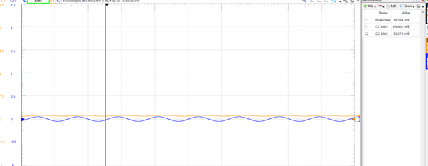
  • The 10 Hz sine case missed the target by a substantial margin.
Documented demonstration measurements
Input and conditionsInput RMSOutput RMSReported errorTrace
Sine · 10 Hz100 mVpp · No DC offset35.27 mV69.86 mV98.18%Outside allowanceView sine test trace
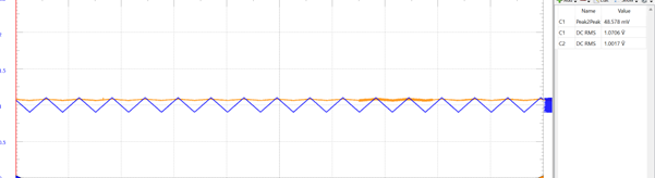
Triangle · 2.5 kHz200 mVpp · 1 V DC offset1.0017 V1.0706 V6.88%Within allowanceView triangle test trace
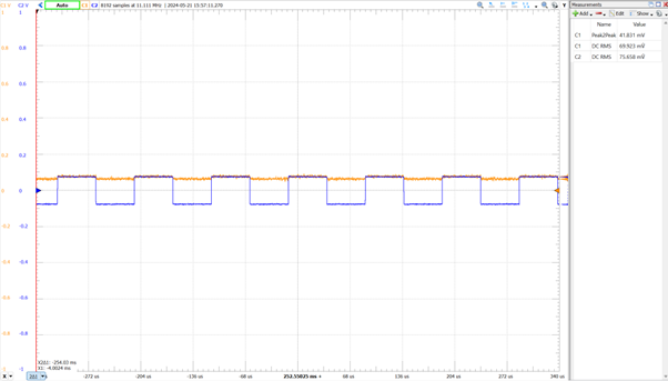
Square · 10 kHz150 mVpp · No DC offset75.66 mV69.92 mV7.58%Within allowanceView square test trace
10 kHz square-wave test

LIMITS REVEALED BY TESTING

A DC output
is only the first check.

  • The low-frequency sine test produced an output, but its magnitude was inaccurate.
  • Offsets and small internal signal levels made calibration important.
  • The selected tests did not establish accuracy across every specified frequency and waveform.
  • The DC-offset test represents one operating case, rather than general AC-plus-DC validation.

08 / REFLECTION

The lessons
I take forward.

  • This project connected circuit theory, simulation and hands-on debugging.
  • It showed how component offsets and interstage signal levels can dominate an otherwise sensible design.
01

Design for the signal at each stage

The square-root circuit needed to handle the filter’s output, rather than the original input amplitude.

02

Make calibration part of the design

Millivolt-level signals made amplifier offsets and adjustable trimming central to practical performance.

03

Test the edges of the specification

The 10 Hz case exposed a limitation that the higher-frequency demonstrations did not reveal.

JERRY SUN / ENGINEERING PORTFOLIO

Back to selected work